You can find the documentation for the opAmp board here:
Inverting network
The inverting network on the Operational Amplifier Experimenter Board, when interfaced with the LT1037 op-amp, plays a crucial role in signal processing. This network is designed to invert the phase of the input signal, meaning that the output signal is 180 degrees out of phase with respect to the input.
Feedback Resistor (Rf): A resistor connected from the output to the inverting input, Rf, plays a pivotal role in determining the gain of the amplifier. The gain in this configuration is given by Rf/Rin , where Rin is the resistor chosen in the inverting input network and the Rf is the resistor chosen in the feedback Network.
Signal Inversion: The primary characteristic of this network is signal inversion, accompanied by amplification based on the resistor values.
What is an Inverting Operation Amplifier?
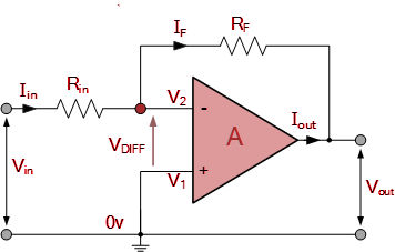
An inverting amplifier utilizes an operational amplifier (op-amp) with two key external components: the input resistor (Rin) and the feedback resistor (Rf). The input signal is applied to the inverting (-) input of the op-amp, while the non-inverting (+) input is typically grounded. The feedback resistor connects the output of the op-amp back to the inverting input. This configuration creates a closed-loop feedback, which is essential for controlling the gain and stability of the amplifier.
The output voltage (Vout) of an inverting amplifier is given by the formula:
Vout=−RinRfVin
where Vin is the input voltage. The negative sign indicates that the output is inverted relative to the input.
Key Features and Advantages
Phase Inversion: The inverting amplifier reverses the phase of the input signal, a characteristic exploited in signal processing tasks such as generating antiphase signals or implementing subtractive mixing.
Adjustable Gain: The gain of an inverting amplifier is easily adjusted by changing the ratio of Rf to Rin, providing flexibility in designing circuits to meet specific amplification needs.
Impedance Matching: These amplifiers can also be used for impedance matching, ensuring maximum power transfer between circuits with differing impedances.
Signal Conditioning: Inverting amplifiers are commonly used in signal conditioning, where signals need to be amplified, filtered, or otherwise modified before being used by the next stage in a system.
Applications
The inverting amplifier configuration finds applications in various areas including, but not limited to:
Audio Electronics: For mixing signals, phase inversion, or creating balanced audio lines.
Analog Computing: Used in operations such as integration, differentiation, and other mathematical functions.
Data Acquisition: To amplify small sensor signals to levels suitable for digitization.
Signal Processing: For dynamic range adjustment, filtering, and constructing active filters.
Instrumentation: In the design of precision measurement devices and systems.
Inverting amplifiers, with their straightforward design and operational flexibility, are indispensable in both educational settings for teaching fundamental electronics concepts and in industry for developing sophisticated electronic systems. Their simplicity, coupled with the vast range of possible applications, underscores the importance of understanding and utilizing inverting amplifiers in the field of electronics and electrical engineering.
💡
Press the on the toggle arrow to extend the theory on Inverting Amplifiers
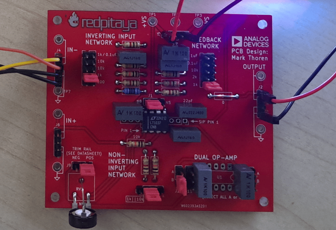
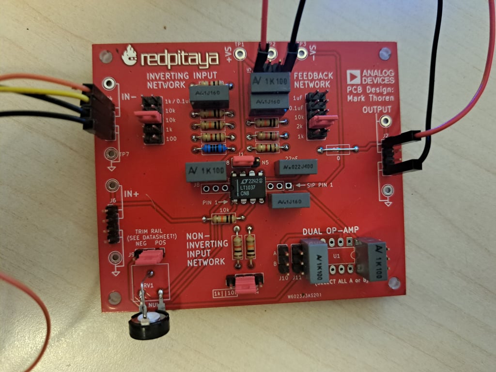
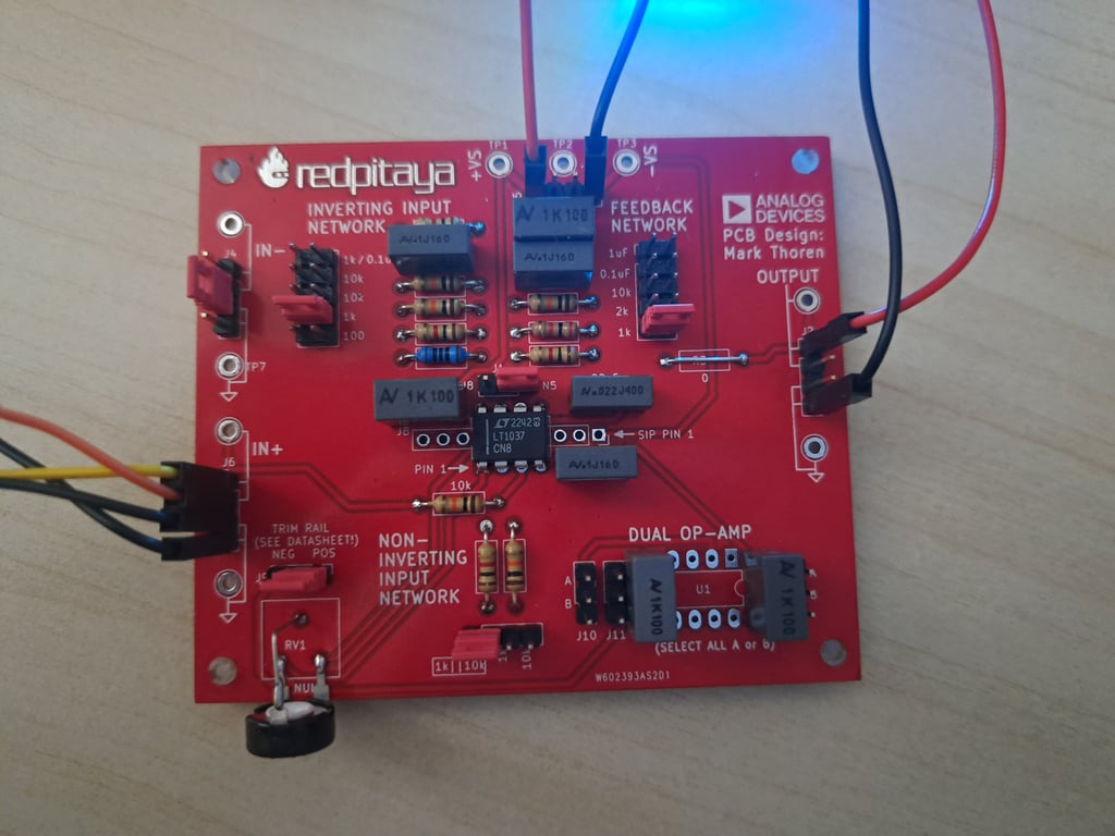
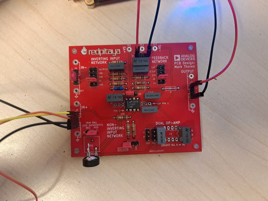
Hardware Setup
A. Materials Required
Red Pitaya STEMlab board
Operational amplifier board in inverting configuration
Oscilloscope probes
Jumper wires
B. Connection Guide
Signal and Power Connections:
Connect the output of the Red Pitaya's signal generator to the IN- terminal on the op-amp PCB (J4 connector).
Move the Bottom jumper 1k||10k to the middle of the connector(pin2,pin3).
Connect the oscilloscope's Channel 1 probe to the same point (IN-) to monitor the input signal to the op-amp.
Connect the oscilloscope's Channel 2 probe to the OUTPUT terminal on the op-amp PCB to observe the amplified signal.
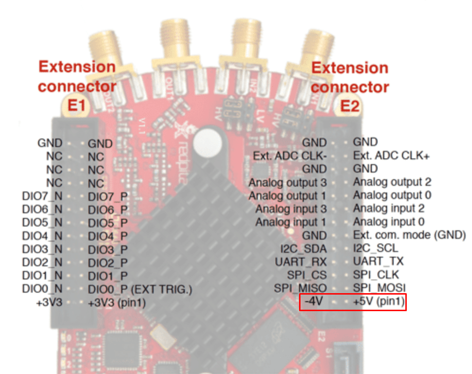
Power the op-amp by connecting the 5V supply from the Red Pitaya to the positive power rail Vs+ and the -4V to the negative power rail Vs- on the op-amp PCB.
Change Ratio of Rin and Rf - By moving the Bridge connectors on the inverting input network, which represents Rin and by moving the bridge connectors on the feedback network, which represents Rf, you can change the gain of the circuit.
Vout=−RinRfVin⟶Au=VinVout=−RinRf
C. Red Pitaya Configuration:
Set up the Red Pitaya's web applications to control the signal generator and oscilloscope.
Set the signal generator to produce a clean sine wave at an initial frequency of 100Hz and an amplitude of 0.1V.
Observe the signal on the Output of the board using the IN2 on the red pitaya oscilloscope app and the Input on the IN1.
Increase the input signal frequency at gain 2 and 10, until you reach 70% of the initial gain which is defined as the -3dB point.
Start with low frequency 100Hz
Increase frequency until you find -3dB Point,
Another measurement at High frequency 20kHz)
*note: in the oscilloscope application, if the auto-scale produces unexpected results try zooming out.
What are decibels[dB]?
Decibels, marked with dB, are a logarithmic unit, used for measuring relative power. To calculate attenuation (or gain) in dB, the following equation is used:
GdB=10⋅log10(P/P0)
If that wasn’t confusing enough, it should be noted that decibels are typically used to compare power, but we will be using them to compare voltages. This is possible because we know that power is proportional to the square of the voltage, and since exponents inside a logarithm translate to multiplication outside of the logarithm, we can use the following equation:
GdB=20⋅log10(U/U0)
Simply put, for every 6 dB, the signal is multiplied (or attenuated) by a factor of two. For example, 30 dB corresponds to 25.
Different gain setting available with picture examples:
Rin=1kOhm, Rf=1kOhm
Au=−(RinRf)=−(11)=−1
Rin=10kOhm, Rf=2kOhm
Au=−(RinRf)=−(102)=−0.5
Rin=1kOhm, Rf=2kOhm
Au=−(RinRf)=−(12)=−2
Conculsion and Results for Inverting Amplifier
Results
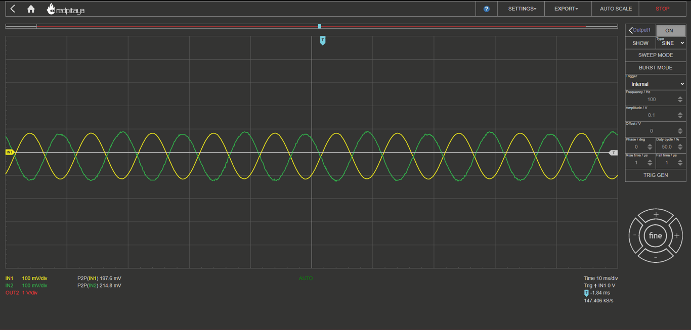
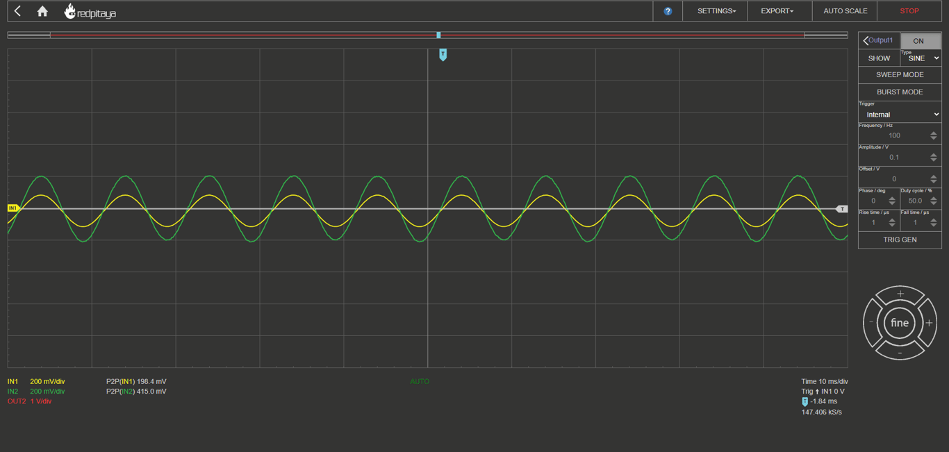
Gain set to 1:
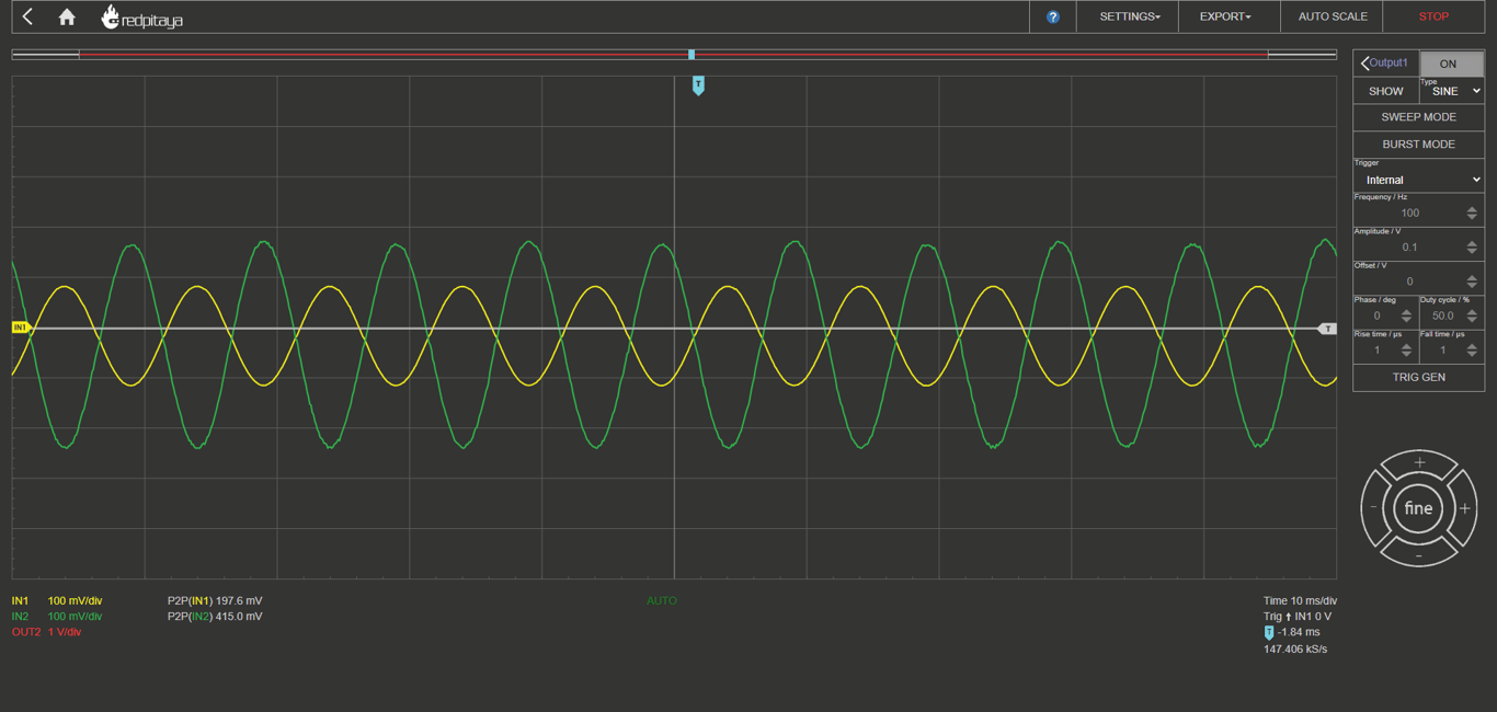
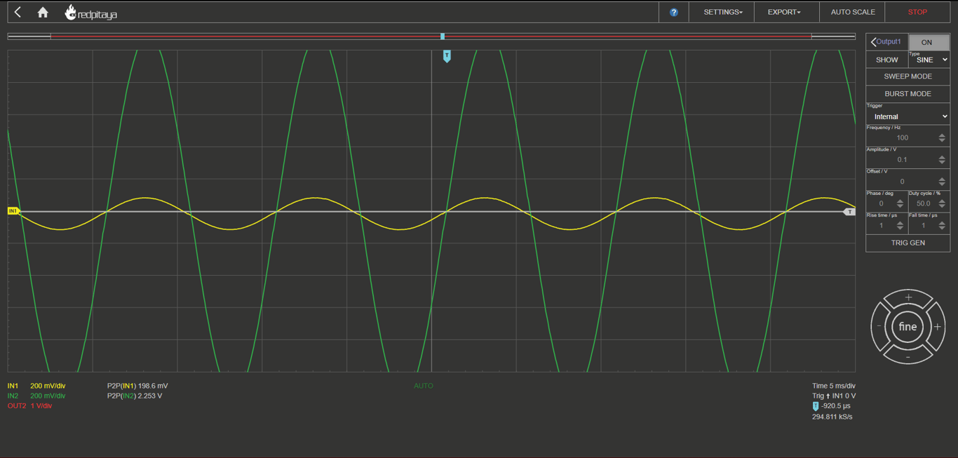
Au=−(RinRf)=−(11)=−1f=100Hz⟶Au≈−1
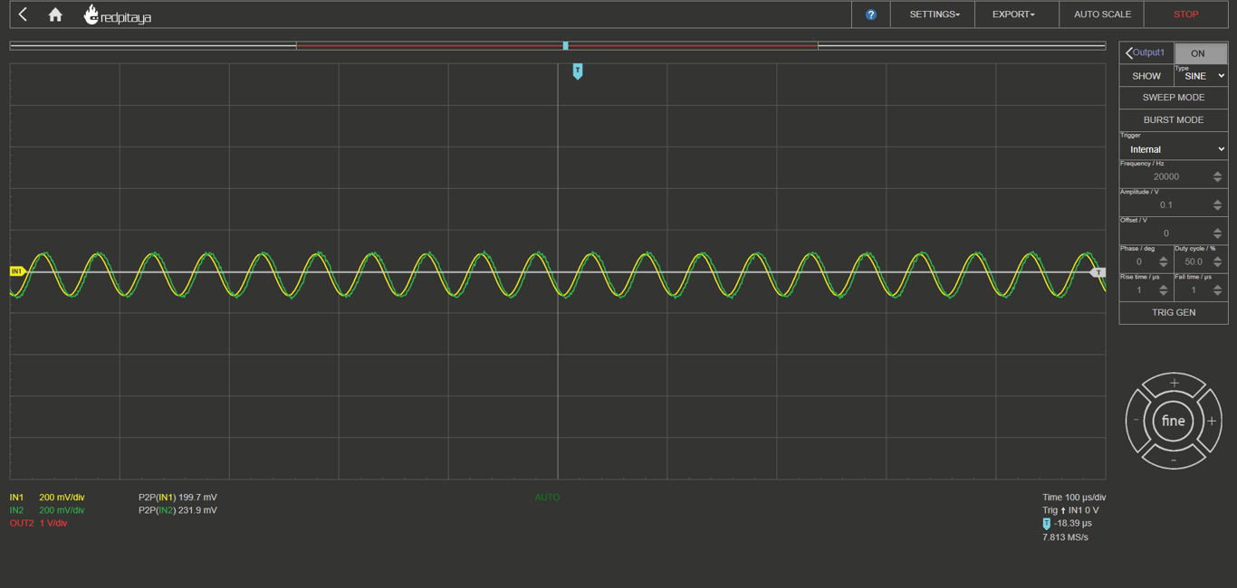
f=8000Hz⟶Au≈−0.7Thisisthe−3dBpoint
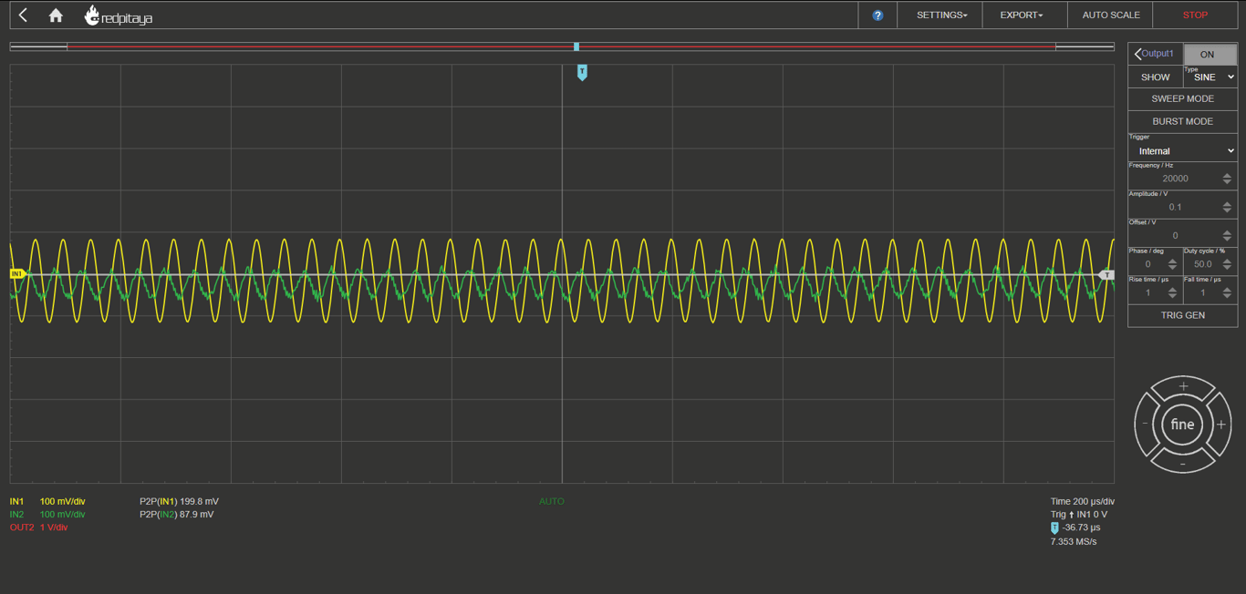
f=20kHz⟶Au≈−0.4
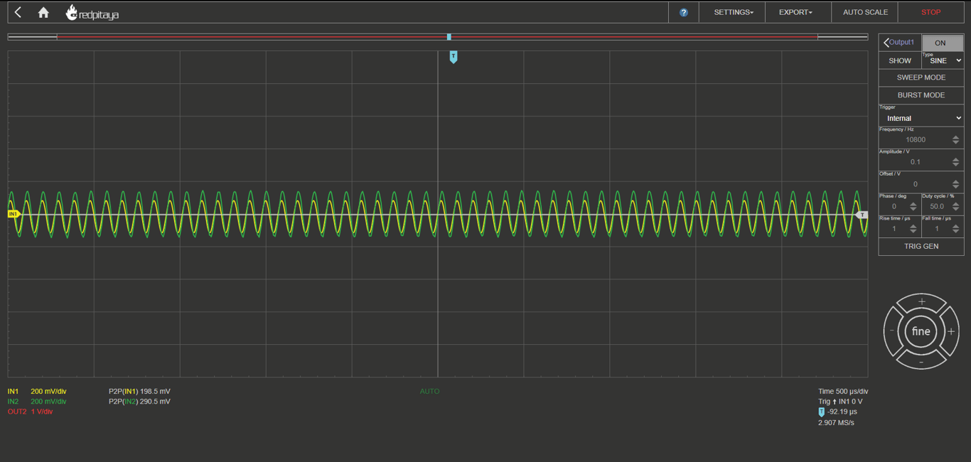
Gain set to 2:
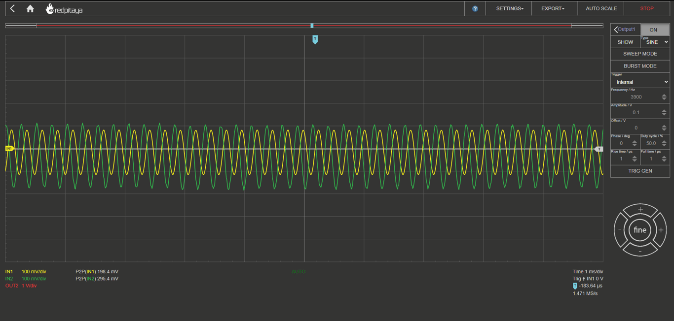
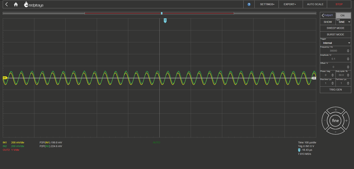
Au=−(RinRf)=−(12)=−2f=100Hz⟶Au≈−2
f=3900Hz⟶Au≈−1.4Thisisthe−3dBpoint
f=20kHz⟶Au≈−0.4
Observations:
Gain Calculations: The gain (Au) for the op-amp in the inverting configuration is computed using the formula Au=−Rf/Rin. Two gain settings are presented: gain set to -1 and gain set to -2, corresponding to the ratios of the feedback resistor to the input resistor.
Low-Frequency Gain: At 100Hz, the output gain closely matches the expected values of -1 and -2 for the respective gain settings, indicating that the op-amp is operating within its linear range at this frequency.
Frequency Response: As the frequency is increased, the magnitude of the gain decreases. For a gain setting of -1, the -3dB point is at approximately 8000Hz, while for the gain setting of -2, the -3dB point occurs at around 3900Hz. This is the frequency at which the gain has decreased by 3dB from its maximum low-frequency value.
Gain at High Frequency (20kHz): At 20kHz, the gain is reduced to approximately -0.4 for both gain settings, showing a significant deviation from the low-frequency gain values.
Commentary:
The experimental data reflect the characteristic behavior of an op-amp in an inverting configuration. The negative gain values are consistent with the inversion of the input signal's phase.
At the fundamental frequency of 100Hz, the measured gains validate the theoretical expectations and suggest that the experimental setup is correctly configured.
The -3dB points highlight the bandwidth limitations of the op-amp. The gain decreases more rapidly at higher frequencies, which is typical for op-amps due to the finite gain-bandwidth product.
At 20kHz, the further reduction in gain illustrates the op-amp's limited ability to amplify signals as the frequency approaches its bandwidth limit. This effect is observed regardless of the initial gain setting.
The drop in gain at higher frequencies can be attributed to the inherent characteristics of the op-amp, such as its open-loop gain and bandwidth. These are significant factors in determining the frequency response of the amplifier.
This experiment demonstrates the critical interplay between gain and frequency in inverting amplifiers and provides empirical data on how an op-amp's gain diminishes with increased frequency.
External factors that could affect the accuracy of these results include the precision of the components (resistors and capacitors), the characteristics of the specific op-amp used, and the measurement equipment's capabilities.
In summary, the experiment effectively illustrates the expected frequency-dependent attenuation of an inverting operational amplifier and provides a clear demonstration of its gain characteristics over a range of frequencies.
Non Inverting Amplifier Experiment
The non-inverting network on the Operational Amplifier Experimenter Board, when used with the LT1037, is integral for applications where phase preservation of the input signal is necessary.
Feedback Loop: A feedback resistor (Rf) is connected from the output to the inverting input, along with a resistor (Rin) connected from the inverting input to the ground. This resistor network sets the gain of the amplifier.
Amplifier Gain: The gain in a non-inverting configuration is given by the formula 1 + Rf/Rin, offering a minimum gain of 1 (unity gain). This allows for signal amplification without inversion.
Phase Consistency: Unlike the inverting configuration, the non-inverting network retains the same phase between the input and output, making it ideal for applications where such consistency is critical.
What is a Non Inverting Amplifier?
Non-inverting amplifiers represent a fundamental configuration in the realm of electronics, characterized by their ability to amplify a signal without inverting its phase. This attribute is particularly advantageous in applications where maintaining the original signal phase is critical. By leveraging an operational amplifier (op-amp) and a simple resistor network, non-inverting amplifiers offer a straightforward yet powerful means for signal amplification, with the added benefit of high input impedance and the ability to control gain precisely.
Operational Principle
The basic setup of a non-inverting amplifier involves an op-amp, a feedback resistor (Rf), and a resistor connected to ground (Rin). The input signal is applied to the non-inverting (+) input of the op-amp, and the inverting (-) input is connected to the output through Rf, forming a feedback loop, with Rin completing the circuit to ground. This configuration ensures that the input and output signals are in phase.
The gain of a non-inverting amplifier can be expressed as:
Vout=(1+RfRin)Vin
This formula indicates that the output voltage (Vout) is directly proportional to the input voltage (Vin), with the gain determined by the ratio of Rf to Rg, plus one.
Key Features and Advantages
Phase Preservation: Unlike inverting amplifiers, non-inverting amplifiers maintain the phase alignment between the input and output signals, an essential feature for many signal processing tasks.
High Input Impedance: The input is applied directly to the op-amp’s non-inverting input, resulting in high input impedance. This makes non-inverting amplifiers ideal for applications where it is crucial to avoid loading the source.
Adjustable Gain: The gain is adjustable and can be set to any value greater than or equal to one, offering flexibility for a wide range of amplification requirements.
Stability and Linearity: The feedback loop contributes to the stability and linearity of the amplifier, making it suitable for high-fidelity and precision applications.
Applications
Non-inverting amplifiers are utilized in a plethora of applications, including:
Buffer Circuits: Serving as a buffer (or unity gain amplifier) to prevent load effects on the source signal.
Signal Conditioning: Amplifying low-level signals to match the input range of analog-to-digital converters.
Audio Amplification: Used in audio equipment to amplify sound signals without altering their phase.
Sensor Signal Amplification: Amplifying outputs from sensors with high output impedance, ensuring that the signal is not degraded before further processing.
Impedance Matching: Facilitating impedance matching between different stages of an electronic system, optimizing power transfer and minimizing signal loss.
The non-inverting amplifier's inherent ability to amplify signals without inverting their phase, combined with its high input impedance and adjustable gain, makes it a versatile tool in the arsenal of electronic circuit design. From simple buffering applications to complex signal conditioning in sophisticated electronic systems, non-inverting amplifiers play a crucial role, underscoring their importance in both academic and practical contexts of electrical engineering and electronics.
💡
Press the on the toggle arrow to extend the theory on Non Inverting Amplifiers
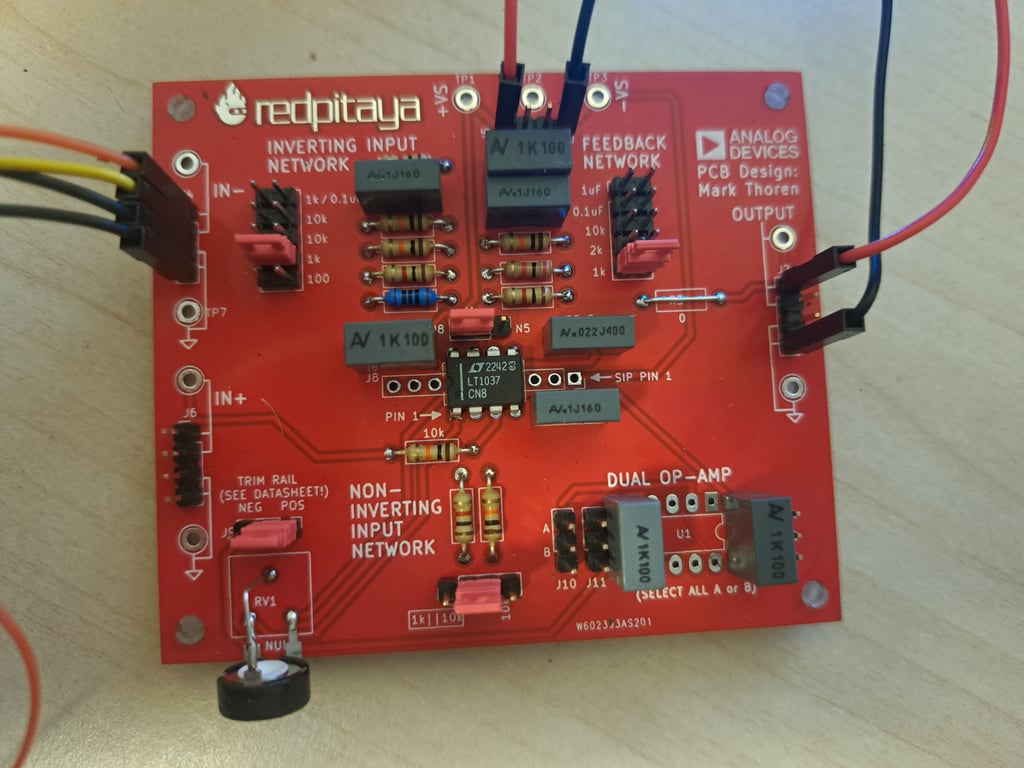
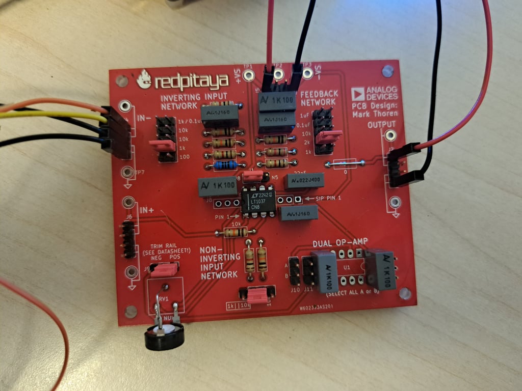
Hardware Setup
A. Materials Required
Red Pitaya STEMlab board
Operational amplifier board in non-inverting configuration
Oscilloscope probes (on the picture yellow and orange jumper are used instead of probes)
Jumper wires
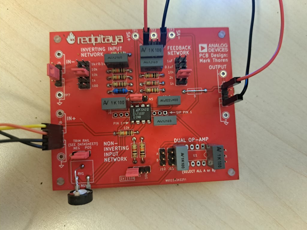
B. Connection Guide
Signal and Power Connections:
Move the Bridge Connector and shortcut the inverting network like shown in the picture bellow. Also move the bottom bridge(non-inverting input) to the left side of the connector.
Connect the Red Pitaya's signal generator output to the IN+ terminal on the op-amp PCB (often marked as the non-inverting input).
Attach the oscilloscope's Channel 1 probe to the IN+ terminal to monitor the input signal. Attach the oscilloscope's Channel 2 probe to the OUTPUT terminal on the op-amp PCB to observe the amplified signal.
Provide power to the op-amp by connecting the 5V and -4V supplies from the Red Pitaya to the appropriate power rails on the op-amp PCB. (same as in inverting configuration)
Change Ratio of Rg and Rf - By moving the Bridge connectors on the inverting input network, which represents Rg and by moving the bridge connectors on the feedback network, which represents Rf, you can change the gain of the circuit.
C. Red Pitaya Configuration:
Set up the Red Pitaya's web applications to control the signal generator and oscilloscope.
Set the signal generator to produce a clean sine wave at an initial frequency of 100Hz and an amplitude of 0.1V.
Observe the signal on the Output of the board using the IN2 on the red pitaya oscilloscope app and the Input on the IN1.
Increase the input signal frequency at gain 2 and 10, until you reach 70% of the initial gain which is defined as the -3dB point.
Start with low frequency 100Hz
Increase frequency until you find -3dB Point,
Another measurement at High frequency 20kHz)els[dB]?
Different gain settings available:
Rg=1kOhm, Rf=1kOhm
Au=(1+RinRf)=(1+11)=2
Rg=10kOhm, Rf=2kOhm
Au=(1+RinRf)=(1+102)=1.2
Rg=1kOhm, Rf=2kOhm
Au=(1+RinRf)=(1+12)=3
Conclusions and Results for Non-inverting Amplifier
Results for Non-inverting Amplifier
Gain set to 2:
Au=(1+RinRf)=(1+11)=2f=100Hz⟶Au≈2
f=10800Hz⟶Au≈1.4Thisisthe−3dBpoint
f=30kHz⟶Au≈1
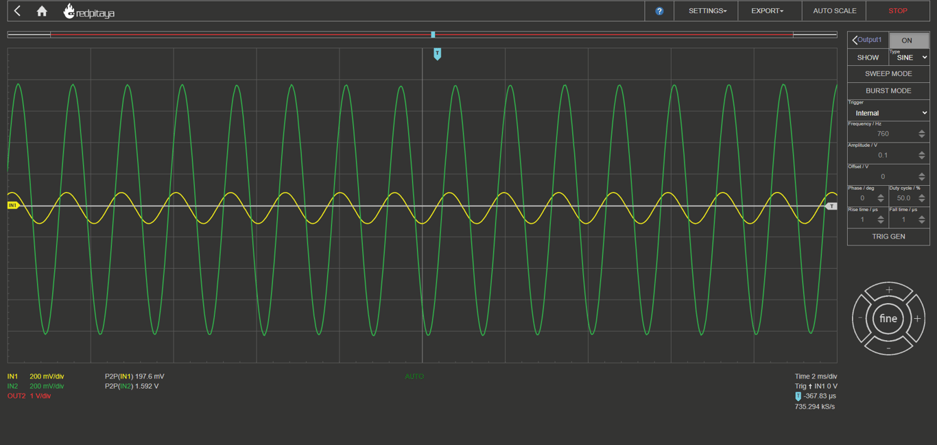
Gain set to 11:
Au=(1+RinRf)=(1+110)=11f=100Hz⟶Au≈11
f=760Hz⟶Au≈8Thisisthe−3dBpoint
f=30kHz⟶Au≈1
Observations:
Gain Settings: There are two gain settings used in the experiments, gain set to 2 and gain set to 10. The gain (Au) has been calculated using the formula Au=1+Rin/Rf for both settings.
Low-Frequency Gain: At a frequency of 100Hz, the gain closely matches the theoretical values calculated for both gain settings (2 for gain set to 2 and 10 for gain set to 10).
High-Frequency Response: As the frequency increases, the gain begins to drop. The point where the gain drops by 3dB from the low-frequency value is referred to as the -3dB point or the cutoff frequency. For a gain of 2, this occurs at approximately 10800Hz, and for a gain of 10, at around 7600Hz.
Commentary:
The results confirm the expected behavior of an op-amp in a non-inverting configuration. The gain at lower frequencies matches the theoretical gain, validating the integrity of the experimental setup and calculations.
The frequency response of the op-amp exhibits the characteristics of a low-pass filter, with the gain remaining constant up to a certain frequency and then rolling off at higher frequencies. This is in line with the standard behavior of operational amplifiers where the gain decreases as the frequency increases due to the limitations of the gain-bandwidth product.
The difference in the -3dB points for the two gain settings suggests that the op-amp has a consistent gain-bandwidth product. As the gain increases, the bandwidth decreases, which is why the -3dB point for a gain of 10 is at a lower frequency than that for a gain of 2.
It is worth noting that the actual -3dB frequency is dependent on several factors, including the specific op-amp model, the feedback network, and the loading effects. Thus, the observed cutoff frequencies are specific to the experiment's conditions and components.
The oscilloscope traces provide a visual confirmation of the frequency response and the effectiveness of the feedback network in controlling the gain. The traces are clean, indicating a stable operation without noticeable noise or distortion within the tested frequency range.
Lastly, it's important to consider the limitations of the experimental setup, including the accuracy of the components (resistors and capacitors, if used), the precision of the frequency generator, and the oscilloscope's resolution. These factors can introduce error into the measurements.
In conclusion, the experiment successfully demonstrates the frequency response of a non-inverting op-amp circuit and the relationship between gain and bandwidth. Further analysis could involve comparing these results with the manufacturer's specifications for the op-amp to determine the accuracy of the measurements.


 Made with Bullet